In 1999, Sony was ascendant. Its video gaming business was its most profitable division, the PlayStation 2 was the world’s most successful console, and hopes were high that the successor would prove even more popular.
To achieve this, the designers believed they would have to make the PlayStation 3 the most powerful console possible, with its own custom microprocessor.
Sony turned to IBM and realized that “there was a potential synergy between the consumer oriented technology that Sony worked on, and the more business and data center oriented technology that IBM worked on,” Peter Hofstee, distinguished researcher at IBM, told DCD.
A year of discussions culminated in a grand vision to develop a radically new chip architecture that the two companies hoped would become integral to consumer electronics, edge devices and data centers.
Behind the Cell
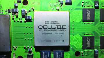
This innovation would be known as the Cell Broadband Engine Architecture, and would help commercialize the concept of heterogeneous computing, which relies on more than one kind of processor or core.
Sony and IBM also recruited Toshiba, which previously worked on the PS2’s Emotion Engine CPU, and together formed the STI Alliance, with a budget of approximately $400 million.
With the Cell chip set to launch as part of the PS3, Sony’s decisions were handled by Ken Kutaragi, the ‘father of the PlayStation’ who was at the time widely expected to become the next Sony president.
“This was research on a development schedule,” Hofstee said. “We did over 600 patents leading into this thing. There were some very significant technical challenges along the way. We would get the architecture team and the key leaders from Sony and Toshiba every morning for weeks, sometimes months on end and we would hash through these things in a very collegial way.”
The principal idea of the chip was to combine a general-purpose Power Architecture core with streamlined coprocessing elements. “One proposal, which maybe does not seem as exciting today, but was pretty aggressive at the time, was a four-core Power proposal. But Kutaragi decided that that was actually not aggressive enough,” Hofstee said.
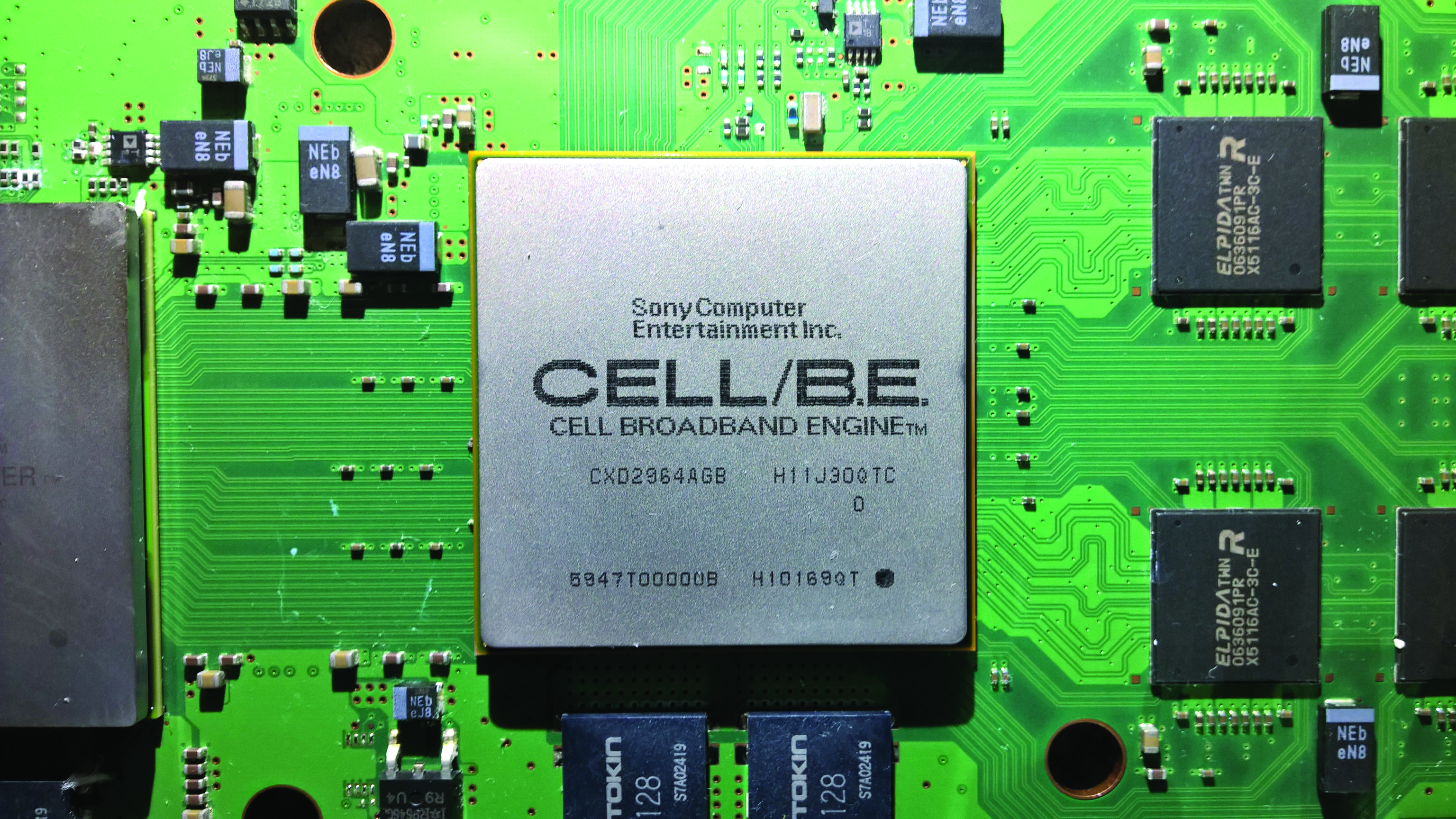
“We ended up with a chip that had nine cores in total - one Power core, and eight Synergistic Processor Elements,” he added. Hofstee was the chief architect of the SPEs, which consisted of a Synergistic Processing Unit (SPU) and a Memory Flow Controller (which had direct memory access, a memory management unit and a bus interface).
Initial plans called for just 64KB of memory for every SPE, but the software team realized very early on that this amount would not suffice. Memory was increased to 128KB, and still, that wasn’t enough. “I said fine by me, but it is a zero sum game, so you can have eight SPEs with 128KB, or six SPEs with 256KB.
“That was when we briefly went from eight to six, then Kutaragi saw that and he said ‘what is this, I didn’t approve that? It has to be eight.’” Later in the meeting, when asked why, he replied: “Eight is a beautiful number.”
“I will never forget that,” Hofstee told DCD.
The PlayStation 3 launched, after some delays, in late 2006 with a 90nm Cell chip inside it. A year later, IBM released the BladeCenter QS21, an energy-efficient server with 1.05 giga–floating point operations per second (GFlops) per watt, and a peak performance of approximately 460 GFlops. Elsewhere, the Cell chip made its way into Mercury Computer Systems servers, Toshiba TVs, Hitachi Medical scanners and Leadtek PCIe cards.
“There were applications for technology in financial services, such as high performance computing for Wall Street, as well as applications for security, oil and gas sectors, gaming and entertainment, and bioinformatics,” Professor David Bader told DCD. “The design was very forward-looking, and the performance improvement was tremendous.”
Bader directed the first Sony-Toshiba-IBM Center of Competence for the Cell Processor, at the Georgia Institute of Technology, which offered training and insights into how to use accelerators and multi-core technologies in data centers.
“This was a chip that was purpose-built for high-end computing as well as gaming systems, that spans the whole gamut of low-end to high-end. It also created a groundswell in the applications space, with new understanding that applications across many sectors, from healthcare to finance to security, could all take advantage of accelerators.”
The machine that could
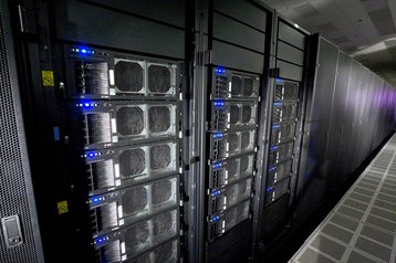
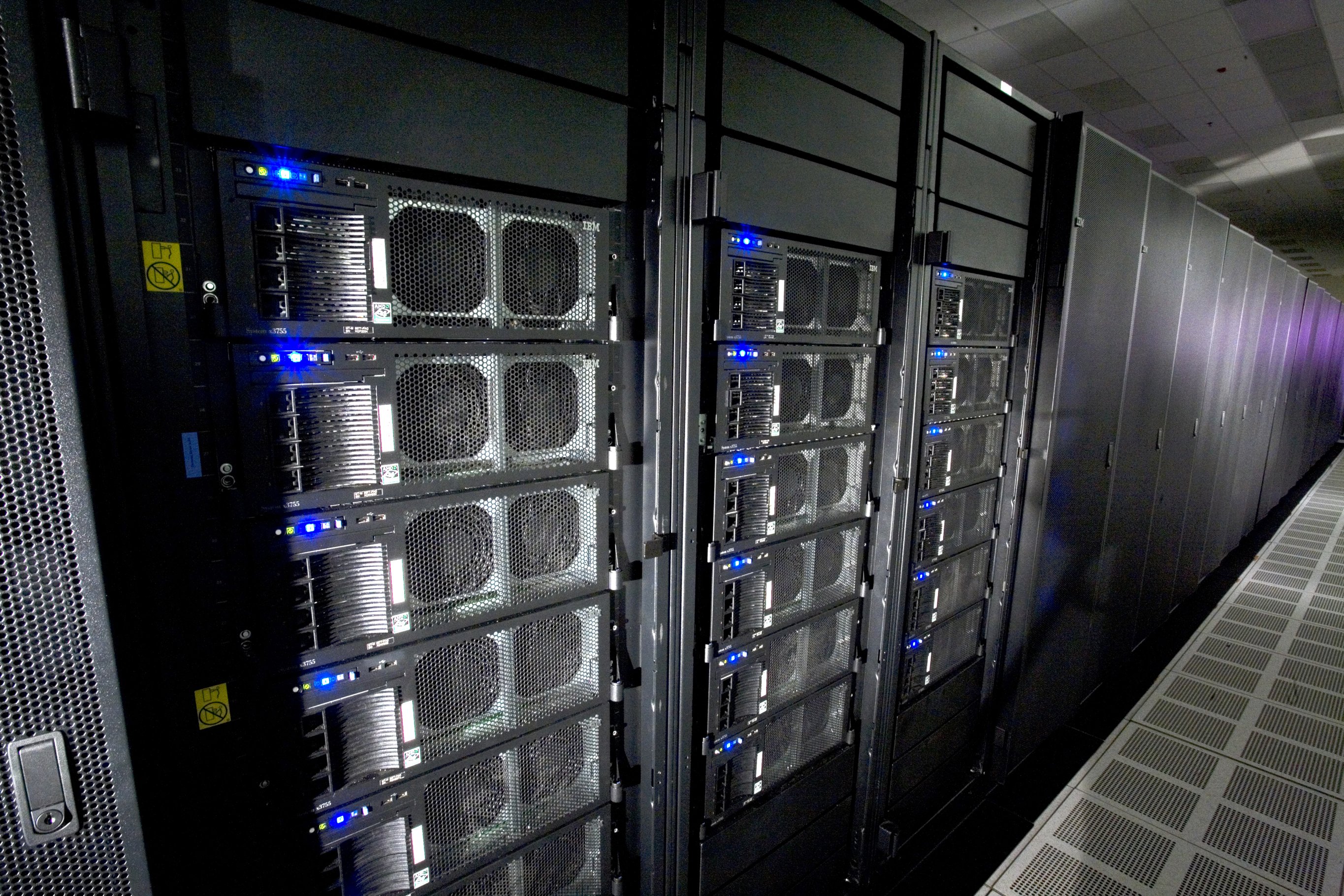
Indeed, IBM did target the high-end computing market: in 2008 it built the world’s most powerful supercomputer to model the decay of the US nuclear arsenal for the Los Alamos National Laboratory. Roadrunner, a $100m system with 12,960 Cell chips (now 60nm with added memory) and 6,480 AMD Opteron dual-core processors, became the world’s first machine to sustain 1.0 petaflops using the Linpack benchmark, roughly double the performance of the next best system.
“In retrospect, if you look at the Top500 chart [a list of the world’s fastest supercomputers], we made quite a step up,” Hofstee said. “You expect a certain growth rate on the list, but you can actually see that the Cell chip jumped off that quite a bit - we held the record a little bit longer than it’s typically held.”
The system was also incredibly energy-efficient, another benefit of the Cell. Hofstee explained: “We went with this philosophy: instead of turning something off when it’s not needed, turning it on only when it is needed.”
The team would run programs and watch which pieces of the chip turned on. “If we would see a floating point unit turn on when the program wasn’t supposed to have a floating point workload, we would know that something’s not quite right. This is an area where people have made more progress since then, but I really think we were the first to adopt this philosophy.”
Bader concurred: “Up to this point in time, when you needed memory, it would be like going to the store and buying a whole case of food and bringing it back, even if you needed just one can. With the Cell, for the first time, you could take a shopping list, go to the store, and fill up your cart just with the individual cans that you may need, and then come home. That was game-changing.”
But, despite the efficiency gains and its high performance, sales of Cell-powered servers were limited. “It was early technology that lacked the set of programmers and programming tools that were readily available for the processor,” Bader said.
“The programming effort to use Cell required skilled and specially-trained programmers. The real challenge is to produce a radically new architecture that’s more efficient and capable while at the same time having the software co-design with programmers who are ready to take advantage of it.”
Hofstee added: “It was fairly difficult for commercial users to adopt Cell if you knew that you had to write your software in such a way that it would only run on Cell. People have to really take a big leap of faith if you’re asking them to do that.
“We were just a tad too early. There were a number of near misses. For example, OpenCL, the open standard for parallel programming of heterogeneous systems, came just too late.”
Hofstee also believes that one could have taken a compiler from supercomputer manufacturer Cray “and retargeted it to a Cell chip, basically by thinking of the local store as a large vector register file.” At the time, he didn’t think there were any open Cray compilers around, but later discovered the Department of Energy had open-sourced one.
“I wish I had known,” he said. “That would have made it more palatable for a community that just couldn’t make a decision to write their future on the architecture.”
Meanwhile, as server sales struggled, Sony’s core consumer product, the PS3, was also in trouble. Initially sold at a significant loss, the console was costing the company billions, its sales lagged behind Microsoft’s Xbox 360, and developers found the unique architecture difficult to make games for. By 2007, Kutaragi had relinquished active management of the business he had built.
“There were plans to have a second generation Cell which was supposed to have 32 SPEs and four Power processing elements, and scale it up,” Professor Gaurav Khanna told DCD.
“What IBM mentioned is that Sony pulled the funding and there were practical reasons for that - Sony had lost a lot of money, they made a lot of investment, the PS3 didn’t quite take traction as quickly as they’d liked. Without Sony funding the next generation, it just died. That’s the hearsay I have heard.”
Unlocking the secrets of the universe
Khanna, a black hole astrophysicist and associate director of the Center for Scientific Computing at the University of Massachusetts Dartmouth, was one of those attracted by the Cell chip’s promise.
His subject of study, while fascinating, is an area “that generally is underfunded simply because there aren’t necessarily very direct practical applications for the research we do, it’s basic research, fundamental physics.”
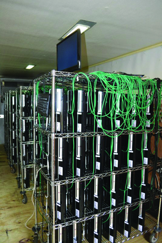
It does, however, require significant computing power to simulate black holes. Short on funding, Khanna had an idea - to use a cluster of PS3s. Not only did they offer a Cell chip at a low price, “Sony made it even easier by offering the possibility of putting Linux on it, and the entire scientific community uses Linux as its bread and butter. It just had to happen, it was such an obvious thing to try to do.”
After contacting Sony because he “couldn’t really go to the National Science Foundation and say ‘give me a couple of thousand dollars for gaming,’” Khanna was given eight consoles by the Japanese corporation and created the Gravity Grid cluster.
“We were able to take those eight machines and show some nice parallel performance, the code soon produced really good results - we even published a paper or two in the first year of this system being built. Then our Dean got interested and he gave us money to double it to sixteen.”
Khanna’s PS3 cluster was the first to lead to published scientific results, although other researchers soon began to build their own. “There are 20 or so papers we’ve published using the cluster at this point,” he said.
And those papers were made possible with an unusually affordable set up. “We did some nice estimates on how much it would have cost with a conventional system, it was easily tenfold. Essentially, one $400 PlayStation was equivalent in performance to 16-32 cores of your several-thousand-dollar Xeon-class x86 server.”
As for energy efficiency, a “PlayStation on full load would consume about 100 watts of power; and at that time a Xeon-class dual socket type server would easily take about a kilowatt. It was quite remarkable.”
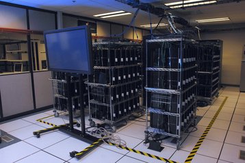
Khanna’s work was not just being watched by other astrophysicists - it also caught the eye of the Air Force Research Laboratory (AFRL), which was eager to explore low power consumption yet high performance chips, especially for use in autonomous drones. “They were quite impressed with the performance of a PlayStation, especially its power efficiency,” he said. AFRL had a lot more resources, and set up a 300 PS3 cluster, which it soon expanded to 1,760 consoles.
From gaming, to warfare
The ‘Condor Cluster’ became the 33rd most powerful supercomputer in the world and ‘the fastest interactive computer in the US Department of Defense,’ capable of 500 trillion floating point operations per second.
AFRL’s director of high power computing, Mark Barnell, said at the time that it cost $2 million, about 5-10 percent of an equivalent enterprise HPC system, and it consumed just 10 percent of the power that one would expect.
Khanna was called in to explain what he had learned from his cluster, and began to help AFRL with their system - in return for access to the hardware.
By late 2012, the Air Force decided to repurpose the floor space, and, with Khanna the Condor’s most active user, he was offered all of the 1,760 systems. After calculating how many the campus could support, he took 400.
“One challenge we had is that they had substantial power and cooling requirements. The bill we had to renovate a lab to house 400 units was more than $500,000,” he said.
“We decided that we had to innovate again, to come up with a crazy idea again.” Khanna looked to markets with large volumes, and found reefer containers - refrigerated units for shipping perishable produce over long distances.

“For $30,000 we had this relatively huge freezer unit that basically gives us cooling capacity of 80,000 British Thermal Units per hour, which is exactly what we needed,” he said.
“At a tenth of the cost, we had a mini data center. That’s what we’ve had now for a couple of years, and the PlayStations have been happily running. We’ve had no trouble, it’s been able to maintain the temperature in a very stable way.”
Khanna’s decade-old system is one of the few remaining implementations of the Cell chip, along with Sony’s PS3 game streaming service, PS Now, which is reported to use racks featuring eight custom console units each (Sony declined to comment). But the impact of the Cell can still be felt elsewhere.
“The heterogeneous computing aspect of that has very much survived,” Hofstee said. “If you look at the supercomputers that IBM is starting to deliver now, the pre-exascale Summit and Sierra supercomputers, it’s Power plus an Nvidia GPU, but I would say it’s very much in the same spirit of Power plus the SPEs that we had on Cell.”
He continued: “I’m very happy with the impact we’ve had on the overall arc of computing architecture.”
As for Bader, he found that the ideas and knowledge produced in the Cell Center made an impact on the broader computing community. Meanwhile, the lessons about software tools and support “really helped provide a commercial success to emerging accelerators such as GPUs, and multi-core technologies.”
He believes that the Cell was “a catalyst, an inflection point between pure CPU computing and moving to accelerators, and understanding the ecosystem required for accelerators, as well as bringing parallel computing to the mainstream.
“Up to that point, every commercial application was single-threaded and the Cell entered the market at a time where developers made the shift to understanding multi-core.”
Khanna added: “Now everyone’s getting back to it, a smartphone System-on-a-Chip has CPU and GPU on the same die. In many ways one could say that the legacy of the Cell is perhaps the most common processor out there.
“I feel bad, really pained that IBM and Sony had this game almost a decade before everybody else got on top of it and sort of dropped it, it’s really painful to see. Maybe the Cell was just too ahead of its time, and now is the time.”
The physicist, meanwhile, was left inspired by the process of turning a consumer product into a data center.
The most recent prototype he has built consists of 32 Nvidia Shield tablets. ”Essentially it is a 16 teraflop system that only uses 300 watts of power, which is almost fivefold more efficient than the most power-efficient supercomputer on Green500, the list of the most efficient HPC systems in the world.“
He told DCD: “We need to misuse more consumer electronics to do science. It’s cheaper for us, it’s more efficient. Why don’t we just piggyback on the innovation that’s happening in consumer electronics?”
This article appeared in the April/May issue of DCD Magazine. Subscribe to the digital and print editions for free here:

