Back in 2011-12, there was a plethora of breakthroughs in silicon-photonic research, with a number of companies claiming big advances, including Intel and IBM, and an expectation that the technology would quickly change the way data centers are built. But a quick search today shows that new information about “lighting up silicon” is almost non-existent. Has the promise not been fulfilled? We asked an expert, Giacomo Losio, head of technology at ProLabs and previously lead optical engineer for Cisco’s transceiver module group.
Can silicon replace glass?
Losio defined silicon photonics as technology that employs silicon (instead of glass) as the light-transport medium. Since silicon is used for integrated circuits, it is conceivable that a hybrid device containing both optical and electronic components could be fabricated on the same substrate — simpler, faster, and all-around better.
However, most fiber-optic/electronic interfaces do not use silicon photonics. Instead, devices use discrete electronics and optics similar to that described by the Fiber-Optic Association:
Electrical signals enter the transmitter and are converted into optical signals (LED or laser). The light from the transmitter then travels through the connected fiber-optic cable. Receiving an optical signal from a connected fiber-optic cable enters the receiver where a detector converts the light into electrical impulses.
This technology has been around for many years and works well. However, the technology is expensive and labor-intensive, due in large part to all the individual electronic components — microchips, amplifiers, drive optics, lasers and photo eyes, to name a few.
For several years, researchers investigated silicon as a way to do away with separate components. However, silicon has several undesirable characteristics. “Silicon is a poor candidate for photonic applications because its electronic structure has an ‘indirect band gap’, making it a poor light emitter,” Mario Paniccia, director of Intel’s photonics technology laboratory, explains to SPIE’s Optics.org. “This means that when an electron and hole combine in silicon, the resulting energy released is more likely to be emitted as vibrational energy, or phonons rather than as photons.”
The trouble with silicon
Silicon afforded researchers at Intel’s photonic lab another stubborn problem: how to modulate optical signals. The material is not known for its ability to change optical properties in response to an electrical field — in technical terms, silicon lacks an electro-optic effect.
Silicon is a poor candidate for photonic applications because its electronic structure has an ‘indirect band gap’, making it a poor light emitter
Mario Paniccia, Intel
The good news is that in 2011, Paniccia and his research team figured out how to overcome silicon being a poor light emitter and not having an electro-optic effect.
The bad news: for years there have been no disruptions, just a few blips on the silicon-photonics marketing radar.
Losio suggests patience: moving from laboratory to beta-testing to production when integrated circuits are involved usually means a five to ten-year development cycle. Unlike discrete components on a PC board, if there is a mistake in the chip design, the prototype chips are scrapped, the design changed, and the entire chip-fabrication process starts over.
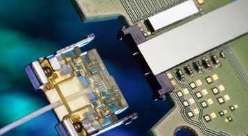
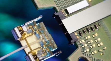
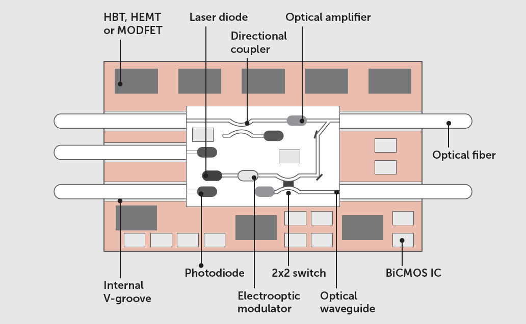
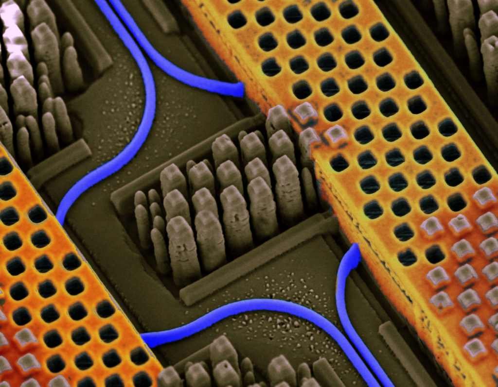
There are some silicon-photonic-based products in the marketplace right now, one of which is the ubiquitous fiber-optic transceiver.
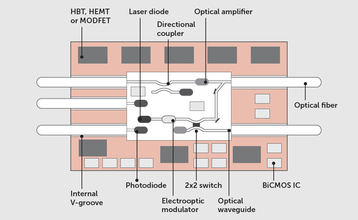
Unlike traditional fiber-optic transceivers using separate components packaged in a hermetically-sealed mechanical assembly, silicon photonic-based transceivers have all the required components on a small integrated circuit, similar to that pictured in the diagram.
Fujitsu appears to be relatively close (early 2017) to releasing its first product using silicon photonics — the Optical PCI Express server. Fujitsu’s Primergy platform and Intel’s optical PCI Express technology showcase new silicon-photonic connections that allow PCI cards to be located away from the motherboard. This affords engineers a great deal of flexibility and should change how servers and racks are designed.
Victor Krutul, director of marketing for the silicon photonics operation at Intel, agrees: “The solution to current power and space density problems is to locate the storage and compute components on a remote blade or tray in such a way that they appear to the CPU to be on the main motherboard.”

Intel’s Rack Scale
Building on the Fujitsu collaboration is Intel’s Rack Scale Architecture introduced in early 2014. Intel threw out the current rack design, coming up with a very different-looking rack based on silicon photonics, that does the following:
- Enables pooled and disaggregated compute, network and storage resources
- Exposes hardware attributes to the provisioning management layer
- Allows software to compose a system based on the requirements of a specific application
- Simplifies cooling and power distribution
Intel and a slew of other companies think silicon photonics will be a disruptive technology, given its potential to commoditize interconnections.
“It also introduces some of the optical features that make dynamic pathing possible in carrier networks,” says Michael Bushong, vice president of marketing at Plexxi. “This allows network architects to provide dynamic bandwidth on a static infrastructure.”
The disruption extends beyond the rack to the data center and to inter data-center communications: “Ultimately, the future of networking has to scale in terms of both performance and cost,” adds Bushong: “And it has to scale across switching, management, and the interconnect. Photonic switching will undoubtedly be the third leg of the commoditization stool.
This article appeared in the April 2015 issue of the DatacenterDynamics magazine