Nvidia has developed a software library for computational lithography, which it believes will massively improve chip design development times, and reduce the number of data centers chip fabs have to rely on.
The Nvidia cuLitho software library is being used by TSMC, the world’s largest contract chip manufacturer, as well as chip design tools company Synopsys and chip manufacturing equipment maker ASML.
The company believes that cuLitho will enable chips with tinier transistors and wires than is now achievable while accelerating time to market and improving the energy efficiency of the data centers that run alongside semiconductor fabs as part of the manufacturing process.
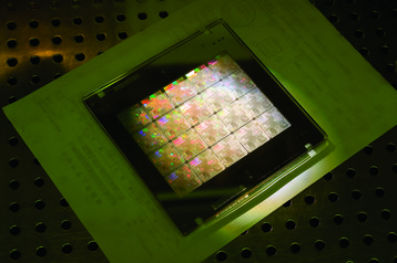
Lithography is the process of creating minute patterns on a silicon wafer, essentially where chip designs created on a computer are physically printed on a piece of silicon.
As transistors have grown smaller, this process has required more and more complex calculations to work out how to operate at such a small scale.
"The calculations became more complicated and required more computers housed in data centers dedicated entirely to computational lithography," Nvidia's Advanced Technology Group VP Vivek Singh said in a press briefing attended by DCD. "These data centers have been growing at a rate faster than Moore's Law. And soon there might not be enough computers in a fab to solve this exploding problem."
Singh added: "If a silicon foundry has three data centers, it'll need 100 data centers by the end of this decade if the trend of the last 15 years continues - that's not feasible. And what about power? 45 megawatts might be okay, but 45 gigawatts? Something's gotta give."
Nvidia claims that the GPU-powered cuLitho solves this conundrum, by delivering a performance leap of up to 40x beyond current lithography, with 500 Nvidia DGX H100 systems able to achieve the work of 40,000 CPU systems.
Fabs using cuLitho may be able to produce 3-5× more photomasks (the templates for a chip’s design) per day, using 9× less power than current configurations. A photomask that required two weeks can now be processed overnight, the company said.
“The chip industry is the foundation of nearly every other industry in the world,” said Jensen Huang, founder and CEO of Nvidia. “With lithography at the limits of physics, Nvidia's introduction of cuLitho and collaboration with our partners TSMC, ASML, and Synopsys allows fabs to increase throughput, reduce their carbon footprint and set the foundation for 2nm and beyond.”
Dr. C.C. Wei, CEO of TSMC, added: “This development opens up new possibilities for TSMC to deploy lithography solutions like inverse lithography technology and deep learning more broadly in chip manufacturing, making important contributions to the continuation of semiconductor scaling.”