Chipmaker NXP has selected AWS as its preferred cloud provider for its electronic design automation (EDA) needs.
The European semiconductor design and manufacturing company is migrating the vast majority of its EDA workloads from NXP data centers and will use AWS infrastructure for its semiconductor design and verification.
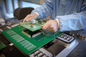
Prior to manufacture, new chips designs undergo testing and validation through the EDA process to ensure they function as expected. NXP said its EDA workflows include front-end design, performance simulation, and verification, along with backend workloads that include timing and power analysis, design rule checks, and other applications in order to prepare a chip for production.
Semiconductor companies typically run EDA workflows from on-premises data centers, but the large compute power involved for each cycle, combined with increasing chip design complexity, means producing a new device can take many months or even years unless companies accurately forecast and install the required compute infrastructure.
NXP said the move will help collaboration while reducing costs and minimizing scheduling risks for design projects.
“Thanks to AWS’s virtually unlimited scale, NXP engineers gain more time to focus on innovation rather than managing compute resources,” the company said.
“We believe cloud-based EDA is critical to accelerating semiconductor innovation and getting new designs to market faster to power an increasingly digital world where more and more devices and infrastructure are connected,” said Olli Hyyppa, CIO and senior vice president, NXP Semiconductors N.V. “We’re excited to expand our relationship with AWS to power the next generation of EDA workloads in the cloud. This will give precious time back to our design engineers to focus on innovation and lead the transformation of the semiconductor industry.”
NXP and AWS have previously announced partnerships around developing cloud solutions for connected cars, and NXP using AWS infrastructure for hosting burst R&D workloads. NXP also provides chips for AWS IoT modules.
“By shifting their EDA workloads to AWS, NXP designers will have access to the best tools available for collaborating on semiconductor design and development around the world,” added Dave Brown, vice president of Amazon Elastic Compute Cloud, Amazon Web Services. “This move will help NXP produce chips that power innovation in IoT, connected cars, and more. We’re proud to support a leading driver of innovation in the semiconductor industry, and we look forward to seeing what becomes possible when chip design moves to the cloud at such a large scale.”


