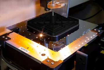
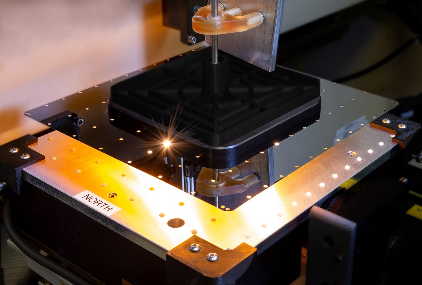
At 15kW, wafer-scale AI prototype will need revolutionary cooling too
The world's largest computer processor has been announced by Cerebras, a company that emerged by stealth this week.
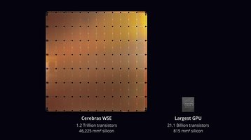
The artificial intelligence chip is a silicon wafer as big as an iPad, and contains 1.2 trillion transistors - about 40 times as many as the most dense processors currently in production, such as AMD's EPYC Rome, which has 32 billion. The Cerebras chip also features 400,000 cores and 18 gigabytes of on-board memory. Intel's recent processors have up to 18 cores.
Cerebras solved fundamental problems that stymied prior attempts to produce wafer-scale silicon, it told the Hot Chips conference at Stanford University this week. Those were the rate of error during manufacturing (yield) and on-chip communications.
Beyond these issues, Cerebras told reporters it also has solutions to the more practical problems which emerge when one thinks about implementing monster chips in systems: packaging, cooling, and thermal expansion. Despite this, the chips are a long way from volume production, and availability in working systems.
400,000 cores
Cerebras designed the chip, called the Wafer Scale Engine, to beat GPUs at AI computing. It replicated the parallel architecture used by GPUs, but took it to the extreme: packing in a massive number of cores, each of which has dedicated memory. Its 400,000 cores are arranged in groups of 4,800, and the groups are arranged on an array of 7x12 tiles. The resulting wafer is 56 times larger than the biggest current Nvidia GPU and consists of a 7x12 array of identical tiles, each of which contains 4,800 cores, each of which has 48 kilobytes of SRAM.
California-based Cerebras made the chip from transistors at a scale of 16 billionths of a meter (nanometers). The most advanced chips in use today have components scaled at half that size. Cerebras has not said what clock speed it operates at, but it is assumed to be comparatively low - less than two or three GHz.
Cerebras developed the WSE quietly with $112 million it got from venture funds including Benchmark. Most of its key staff, including CEO Andrew Feldman and hardware architect Sean Lie, were previously at SeaMicro, an advanced silicon firm bought by AMD.
Electronics manufacturers made similar attempts at wafer-scale integration in the 1980s, but failed because of their yield was too low. Wafers always contain flaws, caused by imperfections in the silicon, and the fine resolution of the photographic lithography production process. Manufacturers cast many chips on a single silicon wafer and discard those found to be flawed when it has broken them off. Most of them will be perfect and usable. But if the whole wafer is used for one processor, it is almost certain to contain dud cores.
Cerebras worked around the problem, by allowing the processor to ignore faulty cores when is operating. It developed communications protocols to solve another problem, which was running data flows between the processor's many tiles. It offering the WSE as a prototypes.
Systems builders must solve other problems to incorporate the WSE into working computers. The chip consumes 15kW of power, which is more than the power consumed by two whole, 6-foot racks of average servers. The only way to remove the heat heat would be to mount the chip vertically, and cool it with a metal plate, with liquid flowing upwards, Feldman has said in interview.
Cerebras announced no production roadmap. But Feldman told EE Times it aimed to match the performance of a thousand Nvidia GPUs using about two percent of the space and power.