The US Department of Commerce has signed a non-binding preliminary memorandum of terms (PMT) to provide Taiwanese silicon wafer supplier GlobalWafers with up to $400 million in proposed direct funding under the CHIPS and Science Act.
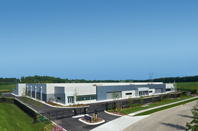
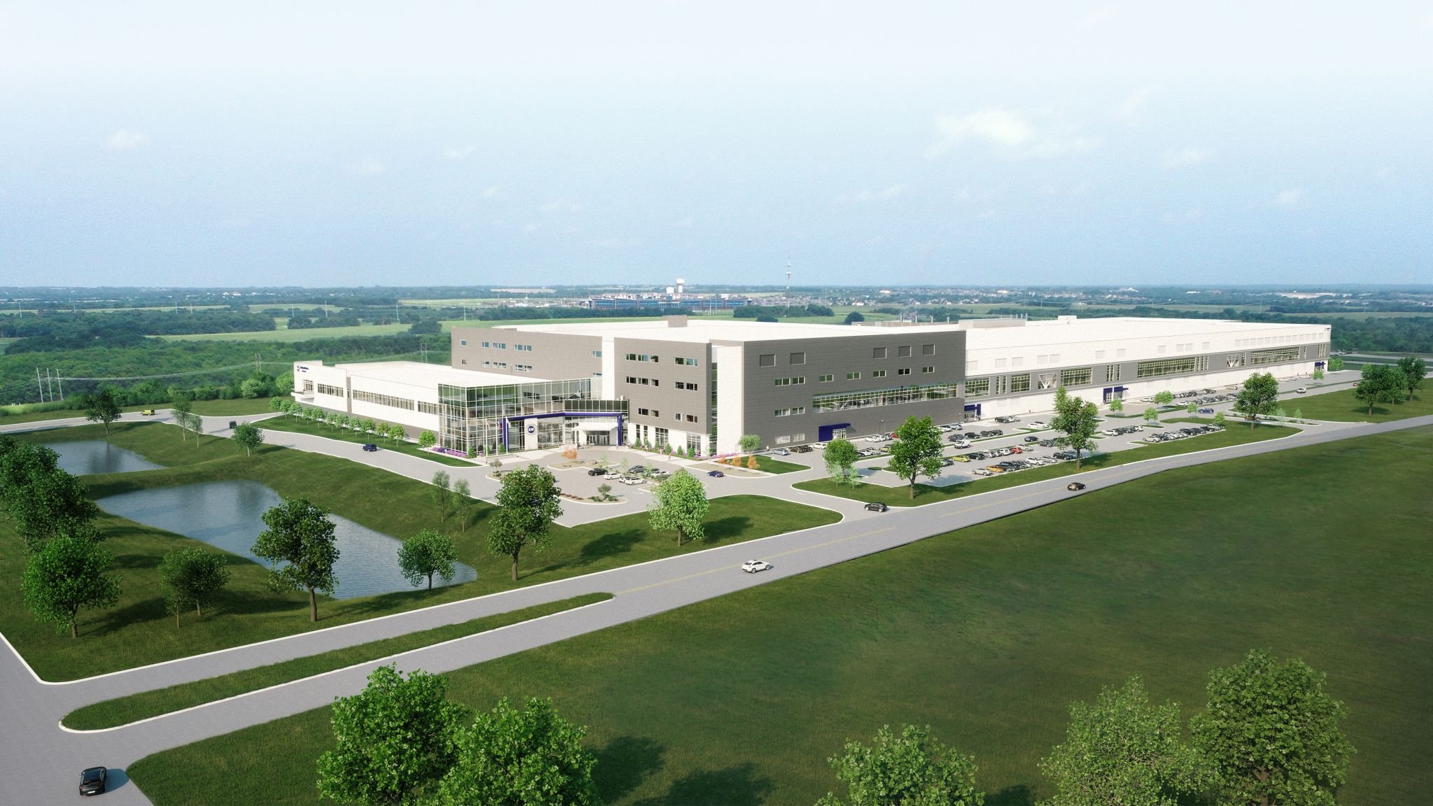
If the agreement moves forward, the funds would be used to establish the US’s first 300mm silicon wafer manufacturing facility for advanced chips in Sherman, Texas.
Part of GlobalWafer’s existing silicon epitaxy wafer manufacturing facility in Sherman would be converted into a silicon carbide (SiC) epitaxy wafer manufacturing site, producing 150mm and 200mm SiC epitaxy wafers.
A second facility in St. Peters, Missouri, would also be built to produce 300mm silicon-on-insulator (SOI) wafers.

According to the department, the investment would create 1,700 construction jobs and 880 manufacturing jobs and support projects with total capital expenditures of approximately $4 billion across both states.
“President Biden is restoring our leadership in the entire semiconductor supply chain – from materials to manufacturing, to R&D. With this proposed investment, GlobalWafers will play a crucial role in bolstering America’s semiconductor supply chain by providing a domestic source of silicon wafers that are the backbone of advanced chips,” said US Secretary of Commerce Gina Raimondo.
“As a result of this proposed investment, the Biden-Harris Administration is helping to secure our supply chains, which will create over 2,000 jobs across Texas and Missouri and ultimately lowering costs and improving economic and national security for Americans.”
In a statement, the Department of Commerce said there are five leading companies, including GlobalWafers, that currently hold over 80 percent of the global 300mm silicon wafer manufacturing market, with approximately 90 percent of silicon wafers sourced today coming from East Asia.
CHIPS Act funding allocations continue to roll out
The $280bn CHIPS and Science Act was approved by Congress in July 2022, with $52bn of the overall funding package designated as subsidies for US semiconductor manufacturers. Funding from the act has also been earmarked for semiconductor R&D, growing a skilled semiconductor workforce, and incentives for the manufacturing of semiconductors and specialized tooling equipment.
In April, Commerce Secretary Gina Raimondo said she expected all the grant money under the CHIPS Act to be allocated by the end of this year.
To date, the White House has allocated the following funding:
- In February 2024, GlobalFoundries was awarded $1.5 billion by the US government under the act to subsidize the company’s future semiconductor production capabilities and support expansion plans for its New York and Vermont sites.
- In March, it was announced that Intel would receive $8.5 billion in direct funding, $11bn in low-interest rate loans, and a 25 percent investment tax credit on up to $100 billion of Intel’s capital investments under the Act. It will be used to support the company’s investments in Arizona, New Mexico, Ohio, and Oregon where the company is expanding its chipmaking facilities.
- In early April, TSMC signed an agreement with the US government in April that would see the company receive $11.6bn under the CHIPS and Science Act to build a third fabrication plant in Phoenix, Arizona. This newly announced TSMC fab will produce 2nm or “more advanced process technologies depending on customer demand” and is expected to be in production by the end of the decade.
- Also in April, it was announced that Samsung Electronics would receive $6.4bn in direct funding to build a semiconductor cluster across a number of locations in Texas. This includes two semiconductor foundries producing 4nm and 2nm chips; an advanced packaging facility for high memory bandwidth; a research and development facility in the city of Taylor, and the expansion of an existing Samsung site in Austin to support the production of fully depleted silicon-on-insulator (FD-SOI) process technologies.
- That same month, Micron was allocated up to $6.14 billion in direct funding under the CHIPS and Science Act, which will be used to support the construction of three new memory chip fabs: Two in Clay, New York, and one in Boise, Idaho, which the company started construction on in 2023. The two fabs in Clay are the first of a planned four-fab “megafab” focused on DRAM (dynamic random-access memory) chip production, while the Boise facility will be a high-volume manufacturing (HVM) fab, also focused on the production of DRAM chips.
- In May, the US government allocated approximately $120 million to Polar Semiconductor to support the expansion and modernization of the company’s manufacturing facility in Bloomington, Minnesota. The investment will allow Polar to double its production of sensor and power chips within two years and introduce new technology capabilities to the site.
- July saw the US Department of Commerce sign a non-binding preliminary memorandum of terms with Rogue Valley Microdevices (RVM) to provide up to $6.7 million in proposed direct funding. Should it be granted, the money would be used to build a pure-play microelectromechanical systems (MEMS) and sensor foundry facility in Palm Bay, Florida, in addition to bolstering the company’s operations in Oregon. RVM is the first women-and minority-owned business set to receive funding under the Act.


