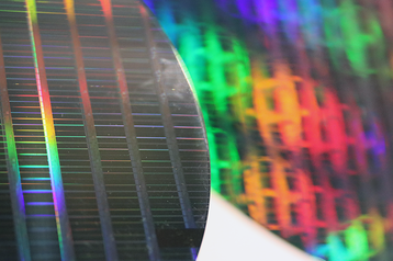
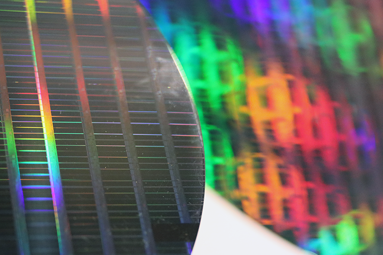
Japanese conglomerate Fujifilm has opened a new facility for the production of Chemical Mechanical Polishing (CMP) slurries, a basic material used in semiconductor manufacturing process.
CMP slurries consist of nano-sized abrasive particles of alumina, silica, and ceria that are dispersed in acidic or basic solutions and used to polish, and ultimately level, the surface of semiconductors.
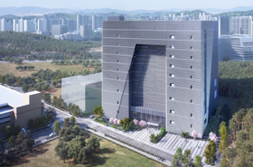
The facility is housed at the company’s display materials site in Kumamoto on Japan's Kyushu island, also known as Fujifilm Material Manufacturing Co. (FFMT Kyushu). Fujifilm Electronic Materials Co. – the company that oversees Fujifilm’s electronic materials business unit – has invested approximately 2 billion yen ($13.6 million) in the site.
The site will produce display and semiconductor materials to shore up the supply of semiconductors in Japan. In addition to this new site in Kumamoto, Fujifilm also has CMP slurries production facilities in Arizona, USA; Cheonan, South Korea; and Hsinchu, Taiwan.
Across its facilities, Fujifilm produces process chemicals that can be used in the pre- and post-processes of semiconductor manufacturing, including photoresists, photolithography-related materials, CMP slurries, post-CMP cleaners, thin-film formation materials, and polyimides.
The company also produces Wave Control Mosaic (WCM) materials such as color filter materials for image sensors. In a statement, Fujifilm said that it plans to start producing color filter material at the FFMT Kyushu site in the spring of 2025.


