Belgian R&D company Imec has reported a number of chip making breakthroughs at the joint lab it runs with EUV lithography company ASML.
According to Imec, it has successfully printed circuit patterns for logic chips with 9.5nm dense metal lines, corresponding to a 19nm pitch and achieving sub-20 nm tip-to-tip dimensions.

Furthermore, the company said it had patterned 2D features at a 22nm pitch, random vias with a 30nm center-to-center distance, and a DRAM-specific layout at a 32nm pitch.
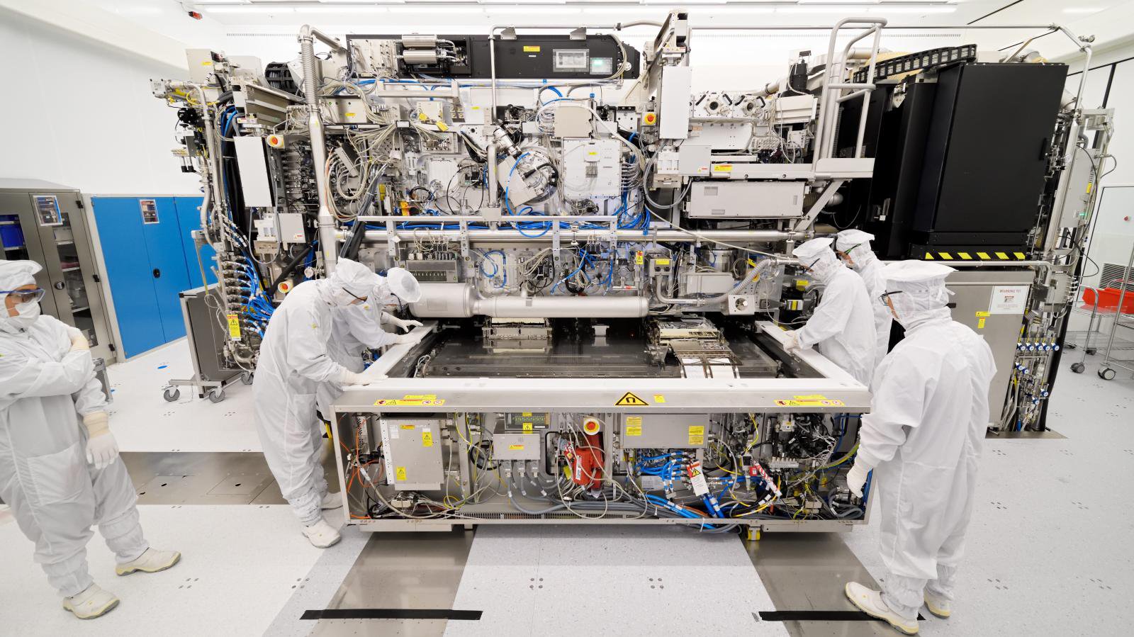
All the breakthroughs were made using a single exposure with materials and baseline processes that have been optimized for ASML’s TWINSCAN EXE:5000 extreme ultraviolet (High NA EUV) scanner, housed at the joint lab in Veldhoven, the Dutch city where ASML is headquartered.
Opened in June 2024, the lab offers companies access to a prototype high numerical aperture High NA EUV scanner, in addition to other tools necessary for the semiconductor manufacturing process, including a coat and development track, metrology tools, and wafer and mask handling systems.
“The results confirm the long-predicted resolution capability of High NA EUV lithography, targeting sub 20nm pitch metal layers in one single exposure,” said Luc Van den Hove, president and CEO of Imec, who added that High NA EUV will be “highly” instrumental to the dimensional scaling of logic and memory technologies.
He added: “These early demonstrations were only possible thanks to the set-up of the joint ASML-Imec lab allowing our partners to accelerate the introduction of High NA lithography into manufacturing.”
ASML is the sole global supplier of extreme ultraviolet lithography photolithography machines that are needed to make the most advanced chips. The company’s standard machines, which were first produced in 2013, have a 0.33NA (numerical aperture), while the High-NA machines have a 0.55NA.
In July, scientists at the Okinawa Institute of Science and Technology claimed they have developed a simplified EUV lithography technology that is superior to the method currently used in semiconductor manufacturing.


