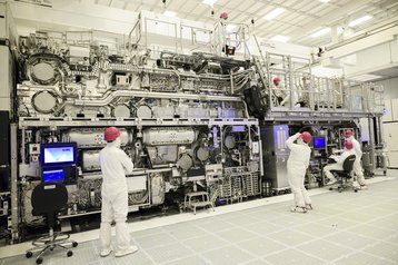
Intel has completed the assembly of its High Numerical Aperture NA Extreme Ultraviolet (High NA EUV) lithography tool at the company’s R&D site in Hillsboro, Oregon.
Built by ASML and delivered in January 2024, the TWINSCAN EXE:5000 is the first commercial lithography system of its kind.
In a statement, Intel Foundry said the tool (also known as 0.55NA EUV) will allow it to deliver new levels of precision and scalability in chip manufacturing, enabling the company to “develop chips with the most innovative features and capabilities that are essential for driving advancements in AI and other emerging technologies.”
When combined with other process technology capabilities being developed by Intel Foundry, the High NA EUV system is expected to be able to print features up to 1.7X smaller than existing EUV tools, enabling 2D feature scaling which will result in up to 2.9X more density.
Unlike traditional 0.33NA EUV, High NA EUV requires less light per exposure, reducing the time required to print each layer, and therefore increasing wafer output.
Intel said it expects to use both 0.33NA EUV and 0.55NA EUV alongside other lithography processes to develop and manufacture its chips, starting with product proof points on Intel 18A in 2025 before moving on to the production of Intel 14A node.
“With the addition of High NA EUV, Intel will have the most well-rounded lithography toolbox in the industry, enabling the company to drive future process capabilities beyond Intel 18A into the second half of this decade,” said Mark Phillips, Intel fellow and director of lithography, hardware and solutions for Intel Foundry Logic Technology Development.
The High NA EUV machine works by hitting droplets of tin heated to approximately 220,000 degrees Celsius (396,032 degrees Fahrenheit) with a laser to create 13.5nm light wavelengths, which do not naturally occur on Earth. This light is then reflected off a mask containing a template of the circuit pattern, and then through an optical system built with the most accurate mirrors ever fabricated.
Intel said it plans to acquire the next-generation TWINSCAN EXE:5200B system from ASML, which can produce more than 200 wafers per hour.
In February 2024, Intel separated its Product and Foundry lines into two separate businesses, rebranding Intel Foundry Services as Foundry and expanding the business unit to include technology development, supply chains, fabrication, and packaging services.
However, earlier this month, the business reported $7 billion in operating losses in 2023 against revenues totaling $18.9bn, a 31 percent decline from the $27.49bn it made in the year prior.
In an attempt to reverse the company’s previous missteps, Intel said it was looking to reduce the total number of outsourced wafers from 30 percent to 20 percent and take full advantage of its High NA EUV machine.


