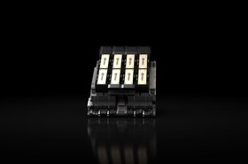
Professor Tsumoru Shintake of the Okinawa Institute of Science and Technology (OIST) has proposed an extreme ultraviolet (EUV) lithography technology that he claims is superior to the method currently used in semiconductor manufacturing.
The method outlined by Shintake and his team uses smaller EUV light sources, which in turn reduces costs and makes the technology more sustainable as it consumes less than one-tenth the power of conventional EUV lithography machines.

Shintake outlined two key challenges with traditional EUV lithography technology that need to be addressed in order to make it more accessible: ensuring efficient light transfer and preventing optical aberrations.
In traditional EUV lithography technology, six mirrors are required, meaning the amount of energy from the original EUV light source that reaches the wafer is around one percent. Shintake’s simplified method requires only two mirrors, meaning the percentage of energy that reaches the wafer is around ten percent.
By optimizing the optical path, the system can operate with an EUV light source of just 20W, leading to a total power consumption of less than 100kW. In contrast, traditional EUV lithography systems often require over 1MW of power.
Shintake said that in order to reduce the number of mirrors from six to two, he had to devise a new method of illumination optics. Dubbed the ‘dual line field,’ it irradiates a flat mirror photomask used in traditional EUV lithography processes without interfering with the optical path.
“OIST is committed to creating cutting-edge science that will impact humanity,” said Gil Granot-Mayer, OIST EVP and leader of OIST Innovation. “This innovation captures the OIST spirit of exploring the impossible and offering original solutions.”
He added: “Although we still have a long way to go in developing this technology, we are committed to doing so. We hope that this technology from Okinawa will have a transformative impact on the semiconductor industry and help solve global issues such as energy consumption and decarbonization."
OIST said it has filed a patent application for this technology and is expecting it to be put to practical use through demonstration experiments.
“The global EUV lithography market is expected to grow from $8.9 billion in 2024 to $17.4 billion in 2030, with an average annual growth rate of approximately 12 percent,” Shintake said. “This patent has the potential to generate tremendous economic benefits.”
Currently, ASML is the sole global supplier of extreme ultraviolet lithography photolithography machines that are needed to make the most advanced 3nm and 5nm chips, however, the company has not remained completely unchallenged.
In October 2023, Canon announced it would be launching a nano-imprint lithography machine that, unlike conventional photolithography equipment which transfers a circuit pattern by projecting it onto the resist-coated wafer, will instead press a mask imprinted with the circuit pattern on the resist on the wafer like a stamp.
Canon claims the machines will be capable of producing parts down to a 5nm node, and could eventually produce 2nm nodes once the technology has been refined even further. Additionally, by removing the need for an optical mechanism, Canon said it will be able to reduce the cost of ownership of machines.


