Photonics startup Lightium has secured $7 million in seed funding to commercialize its lithium niobate-based photonic chips.
The round was co-led by Vsquared Ventures and Lakestar. The Swiss company said the funding will accelerate the development and manufacturing of photonic chips.
Lightium’s technology uses a glass material called thin-film lithium niobate (TFLN) that the company says overcomes traditional semiconductor transceiver limitations by increasing transmission bandwidth and reducing energy consumption.
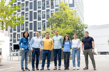
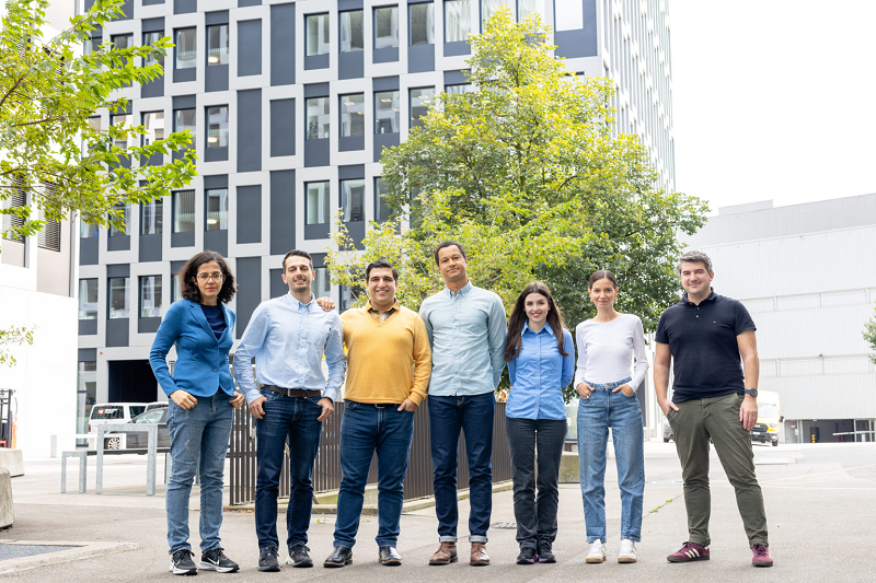
Founded last year by Dr. Amir Ghadimi, Dr. Frédéric Loizeau, and MIT professor Prof. Dirk Englund, Lightium said its products could offer data rates of 1.6 to 3.2Tbps.
Dr. Ghadimi, CEO of Lightium, said: “Current semiconductor-based technologies that are powering data centers have reached their limits - they cannot run faster or more efficiently. Lightium uses TFLN to solve this problem and we have now developed the manufacturing capability to provide this technology at scale for the industry. What used to be limited to academic and R&D cleanrooms has now become an accessible reality for the industry to adopt.”
However, TFLN is a difficult material to process and has, up to now, been restricted to prototyping in academic and R&D settings. Lightium's proprietary manufacturing process aims to enable volume production.
Dr. Jakob Lingg, investment manager at Vsquared, added: "Optical communication companies have clear roadmaps for future data transmission and energy requirements. As silicon struggles to meet these demands, there is a strong market pull for alternative materials with superior electro-optical properties."
Steven Jacobs, Lakestar partner and CPO, said: “By transitioning from silicon photonics, which have reached the physical limits of their material properties, to TFLN, which can scale for the foreseeable future, Lightium enables data centers to increase their speeds 10x or more. At the same time, because of how efficient TFLN is, it can lower data center operating costs, which are primarily tied to energy consumption.”
Lightium said its TFLN platform can be used in satellite communication, quantum computing, novel optical computing architectures, and LIDAR applications.
Over the next year, Lightium will enhance its manufacturing, design, and testing capabilities, optimize its Process Design Kit (PDK), and expand its partnership network to support wide-scale commercialization.
Currently in a closed beta run with strategic partners, Lightium aims to launch its foundry services at the beginning of 2025. On its website, the company said it manufactures 200 mm wafers.
InnoSuisse, the Swiss Innovation Agency, awarded Lightium a 2.67 million CHF ($3.1m) grant earlier this year.


