We all know that liquid cooling is the future for data centers. Air simply can’t handle the power densities that are arriving in data halls, so dense fluids with a high heat capacity are flowing in to take over.
As the heat density of IT equipment increases, liquids have inched ever closer to it. But how close can the liquids get?
Running a water-circulating system through the rear doors of data center cabinets has become well-accepted. Next, systems have been circulating water to cold plates on particularly hot components, such as GPUs or CPUs.
Beyond that, immersion systems have sunk whole racks into tanks of dielectric fluid, so the cooling liquid can contact every part of the system. Major vendors now offer servers optimized for immersion.
But there is a further step. What if the fluid could be brought closer to the source of that heat - the transistors within the silicon chips themselves? What if coolants flowed inside processors?
Husam Alissa, a director of systems technology at Microsoft, sees this as an exciting future option: “In microfluidics, sometimes referred to as embedded cooling, 3D heterogenous, or integrated cooling, we bring the cooling to the inside of the silicon, super close to the active cores that are running the job.”
This is more than just a better cooling system, he says: “When you get into microfluidics, you're not only solving a thermal problem anymore.” Chips with their own cooling system could solve the problem at the source, in the hardware itself.
Birth of microfluidics
In 1981, researchers David Tuckerman and R F Pease of Stanford suggested that heat could be removed more effectively with tiny “microchannels” etched into a heatsink using similar techniques to those used in silicon foundries.
The small channels have a greater surface area and remove heat more effectively.
The heatsink could be made an integral part of VLSI chips, they suggested, and their demonstration proved a microchannel heatsink could support a then-impressive heat flux of 800W per sqm.
From then on, the idea has persisted in universities but only tangentially affected real-life silicon in data centers.
In 2002, Stanford professors Ken Goodson, Tom Kenny, and Juan Santiago set up Cooligy, a startup with an impressive design of “active microchannels” in a heatsink built directly onto the chip, along with a clever silent solid-state electrokinetic pump to circulate the water.
Cooligy’s ideas have been absorbed by parts of the mainstream. The company was bought by Emerson Network Power in 2005. Its technology, and some of its staff, still circulate in Emerson’s new incarnation, Vertiv.
The idea of integrating cooling and processing became more practical as silicon fabrication developed and went into three dimensions. Starting in the 1980s, manufacturers experimented with building multiple components on top of each other on a silicon die.
Making channels in the upper stories of a multi-layer silicon chip is potentially a quick win for cooling, as it can start simply by implementing tiny grooves similar to the fins seen on heatsinks.
But the idea didn’t get much traction, as silicon vendors wanted to use 3D techniques to stack active components. That approach is now accepted for high-density memory, and patents suggest that Nvidia may be intending to stack GPUs.
In the microprocessor industry, cooling and processing were seen as separate disciplines. Chips had to be designed to dissipate their heat, but this was done by relatively unsophisticated means, using thermal materials to siphon the heat to the big copper heatsink on the surface.
The heatsink could be improved by etching smaller channels, but it was a separate item, and heat had to cross a barrier of adhesive to get there.
But some researchers could see the possibilities. In 2020, Tiwei Wei, of the Interuniversity Microelectronics Centre and KU Leuven in Belgium, integrated cooling and electronics in a single chip.
Wei, whose work was published in Nature in 2020, did not think the idea would catch on in microprocessors, saying that micro cooling channels would be more useful in power electronics, where large-sized chips made from semiconductors like gallium nitride (GaN) actually manage and convert electricity within the circuits.
That possibly explains why Emerson/Vertiv wanted to get hold of Cooligy, but Wei didn’t see the tech going further: “This type of embedded cooling solution is not meant for modern processors and chips like the CPU,” he told IEEE Spectrum.

Digging into the chips
Already, by that time, researchers had been working on etching microfluidic channels into the surface of silicon chips for some years. A team at Georgia Tech working with Intel in 2015 may have been the first to make FPGA chips with an integrated microfluidic cooling layer, on top of the silicon, “a few hundred microns [micrometers] away from where the transistors are operating.”
“We have eliminated the heat sink atop the silicon die by moving liquid cooling just a few hundred microns away from the transistor,” team leader Georgia Tech Professor Muhannad Bakir said in Georgia Tech’s press release. “We believe that reliably integrating microfluidic cooling directly on the silicon will be a disruptive technology for a new generation of electronics.”
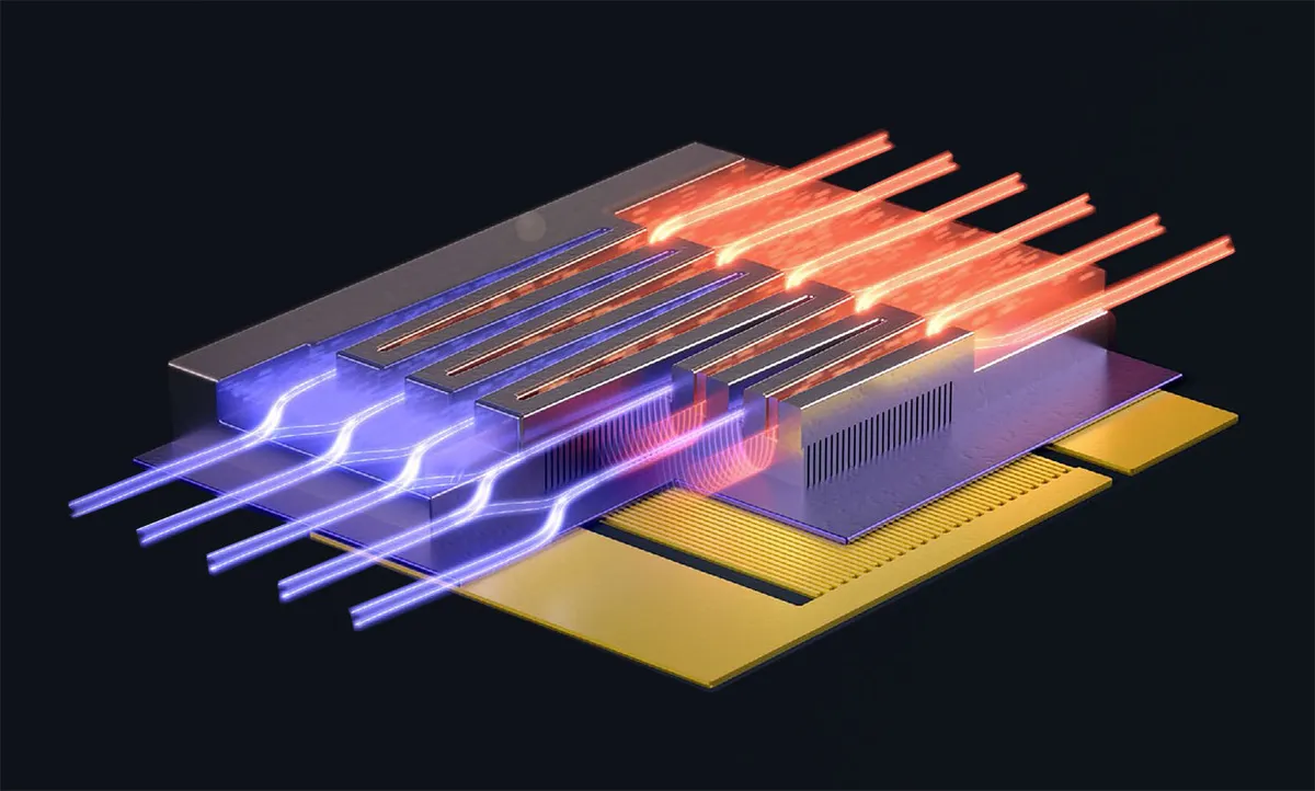
In 2020, researchers at the École Polytechnique Fédérale de Lausanne in Switzerland, took this further, actually running fluid in tunnels underneath the heat-generating transistors.
Professor Elison Matioli saw the opportunity to bring things even closer together: “We design the electronics and the cooling together from the beginning,” he said in 2020, when his team’s paper was published in Nature.
Matioli’s team had managed to engineer a 3D network of microfluidic cooling channels within the chip itself, right under the active part of each transistor device, just a few micrometers away from where the heat is produced. This approach could improve cooling performance by a factor of 50, he said.
Matioli etched micrometer-wide slits in a gallium nitride layer on a silicon substrate, and then widened the slits in the silicon substrate to form channels that would be big enough to pump a liquid coolant through.
After that, the tiny openings in the gallium nitride layer were sealed with copper, and a regular silicon device was created on top. “We only have microchannels on the tiny region of wafer that’s in contact with each transistor,” he said at the time. “That makes the technique efficient.”

Matioli managed to make power-hungry devices like a 12kV AC-to-DC rectifier circuit which needed no external heatsink. The microchannels took fluid right to the hotspots and handled incredible power densities of 1.7kW per sq cm. That is 17MW per sqm, multiple times the heat flux in today’s GPUs.
On to standard silicon
Meanwhile, work continues to add microfluidics into standard silicon, by creating microfluidics structures on the back of existing microprocessors.
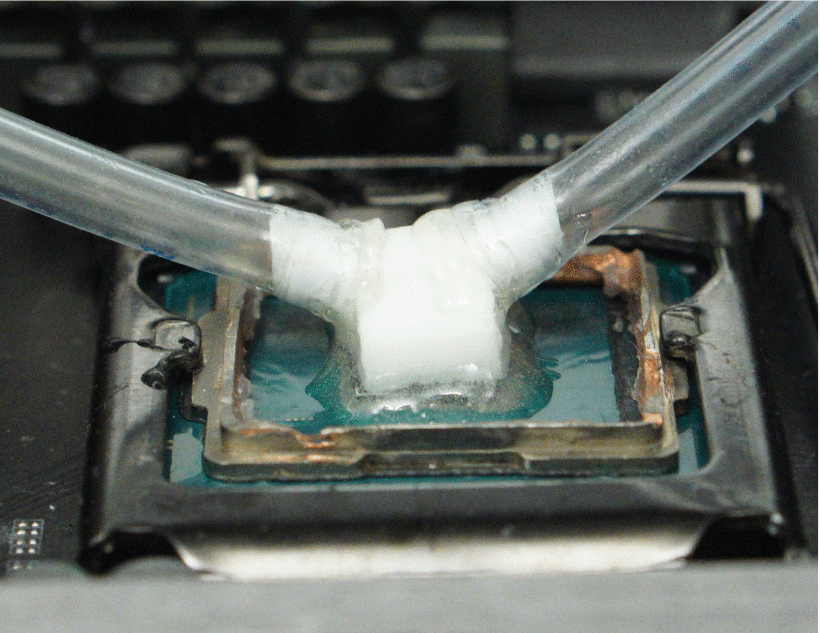
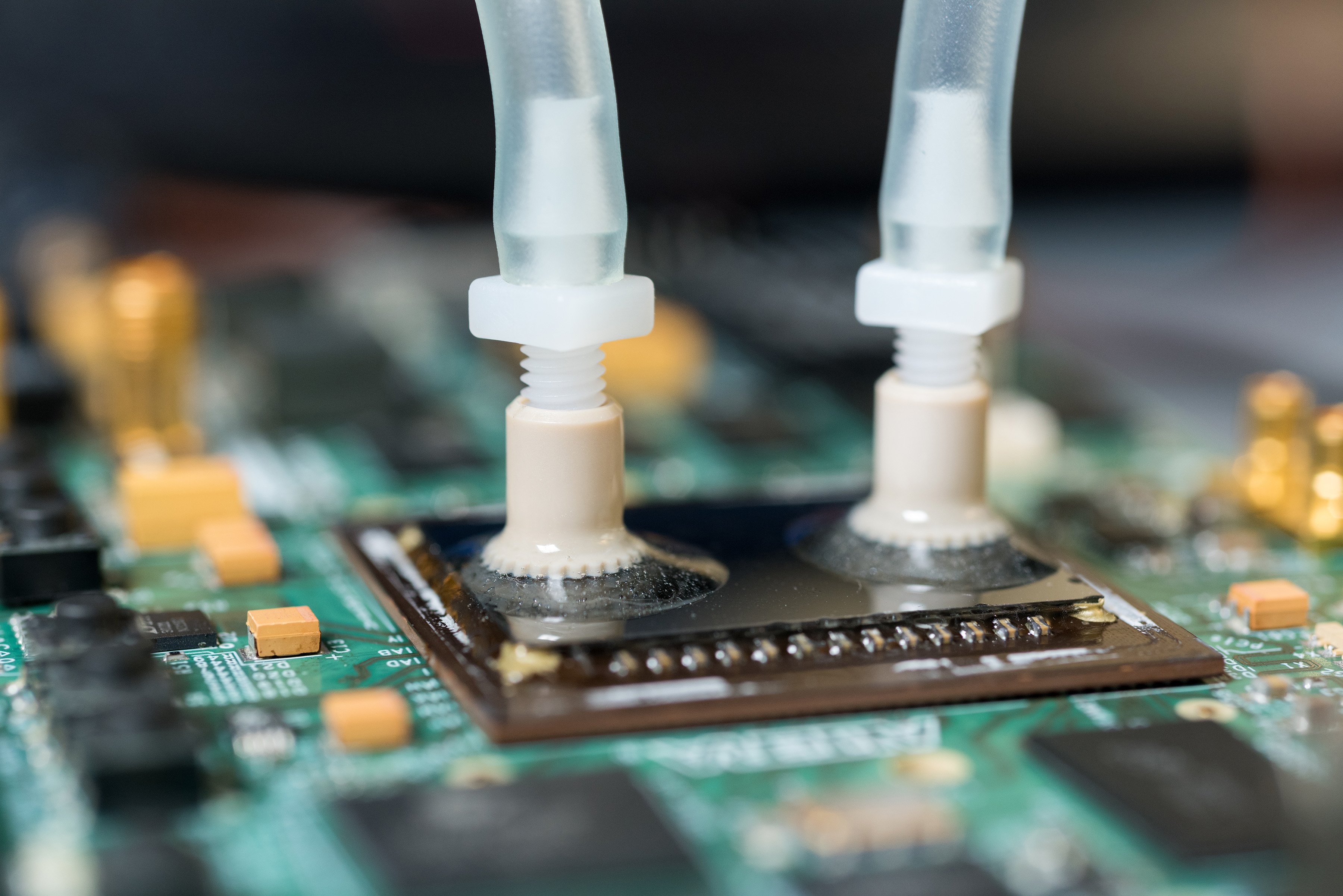
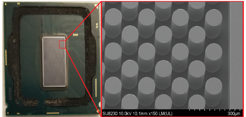
In 2021, a Microsoft-led team, including Husam Alissa, used “micropin” fins etched directly on the backside of a standard off-the-shelf Intel Core i7-8700K CPU.
“We actually took an off-the-shelf desktop-class processor, and removed the case,” he says. Without the heat spreader cover and the thermal interface material (TIM), the silicon die of the chip was exposed.
“When that die was exposed, we applied etching methods to carve out the channels that we want to see,” he continues. The back of the die was etched away selectively, to a depth of 200 microns, leaving a stubble-field pattern of rods 100 microns thick - the “micropins” that form the basis of the integral direct-to-chip cooling system.
That’s a delicate task, warns Alissa: “You have to consider how deep you are etching, so you are not impacting the active areas of the silicon.”
Finally, the back of the CPU die was sealed in a 3D-printed manifold, which delivered coolant to flow amongst the micropins. The chip was then overclocked to dissipate 215W of power - more than double its thermal design power (TDP), the energy it is designed to handle safely without overheating.
Surprisingly, the chip was able to perform at this level using only room-temperature water. Delivered through the manifold. The experiment showed a 44 percent reduction in junction-to-inlet thermal resistance and used one-thirtieth the volume of coolant per Watt than would have been needed by a conventional cold plate. The performance was evaluated with standard benchmark programs.

This was the first time microfluidics channels were created directly on a standard consumer CPU and achieved the highest power density with microfluidic cooling on an active CMOS device. The results show the potential to run data centers more efficiently without the need for energy-intensive refrigeration systems, the group reported in IEEE Xplore.
All that would be needed would be for the chip maker to mass-produce processors with etched micropins, and sell them packaged with a manifold attached in place of the usual heatspreader cap.
If foundries like TSMC could provide their chips with built-in liquid cooling, that would change the dynamics of adoption. It would also allow the technology to push boundaries further, says Alissa.
“With cold plates, you might get water at 40°C (104°F) but with microfluidics you could probably have 80°C (176°F) and higher coming out of these chips, because the coolant is so close to the active cores,” he says. “This obviously enhances the efficiency and heat recovery benefits, paired with lower requirements for flow rate.”
The future of microfluidics
“There are two main flavors of microfluidics,” says Alissa. The lighter touch option, which he says could be deployed “in a couple of years,” is the approach his team showed - to etch channels in commercial chips: “Go buy chips, do the etching, and you're done.”
A more fully developed version of this approach would be for the foundries to do the etching before the chip reaches the consumer - because not everyone wants to lever the back off a processor and attack it with acid.
Beyond that, there is what Alissa calls the “heavier touch” approach. In this, you “intercept early at the foundry and start building 3D structures.” By this, he means porous chips which stack components on top of each other with coolant channels in the layers between.
That’s a development based on the approach used by Matioli in Lausanne. As Alissa says, “That promises more but, obviously, it's more work.”
Alissa has a goal: “The North Star we want to get to is where we're able to jointly optimize this chip for cooling and electrically at the same time, by stacking multiple dies on top of each other, with [microchannel] etching in between.”
Cooling would allow multiple components to be stacked and connected “through chip vias” (TCVs) which are copper connections that travel through the silicon die. These tower chips could need lower energy and work much faster, as the components are closer together: “Overall, you're gaining on performance, you're getting on cooling, and also on latency because of the proximity.”
There’s another benefit. If microfluidics allows chips to go to a higher thermal design point (TDP) this could remove one of the hurdles currently facing silicon designers.

The Future of Cooling
Preparing for a high-density data center
The difficulty of removing heat means that today's largest chips cannot use all their transistors at once, or they will overheat. Chips have areas of “dark silicon” (see box), and applying microfluidics could allow designers to light those up, boosting chip performance.
But don’t expect microfluidics to solve everything. Back in 2012, Professor Nikos Hardavellas (see box) predicted the next problem: “Even if exotic cooling technologies were employed, such as liquid cooling coupled with microfluidics, power delivery to the chip would likely impose a new constraint.”
Once we work out how to get more heat off the chip, we will have to develop ways to deliver a large amount of power, that can provide signal integrity at the low voltages required by the transistors.
Are we ready for that one?


