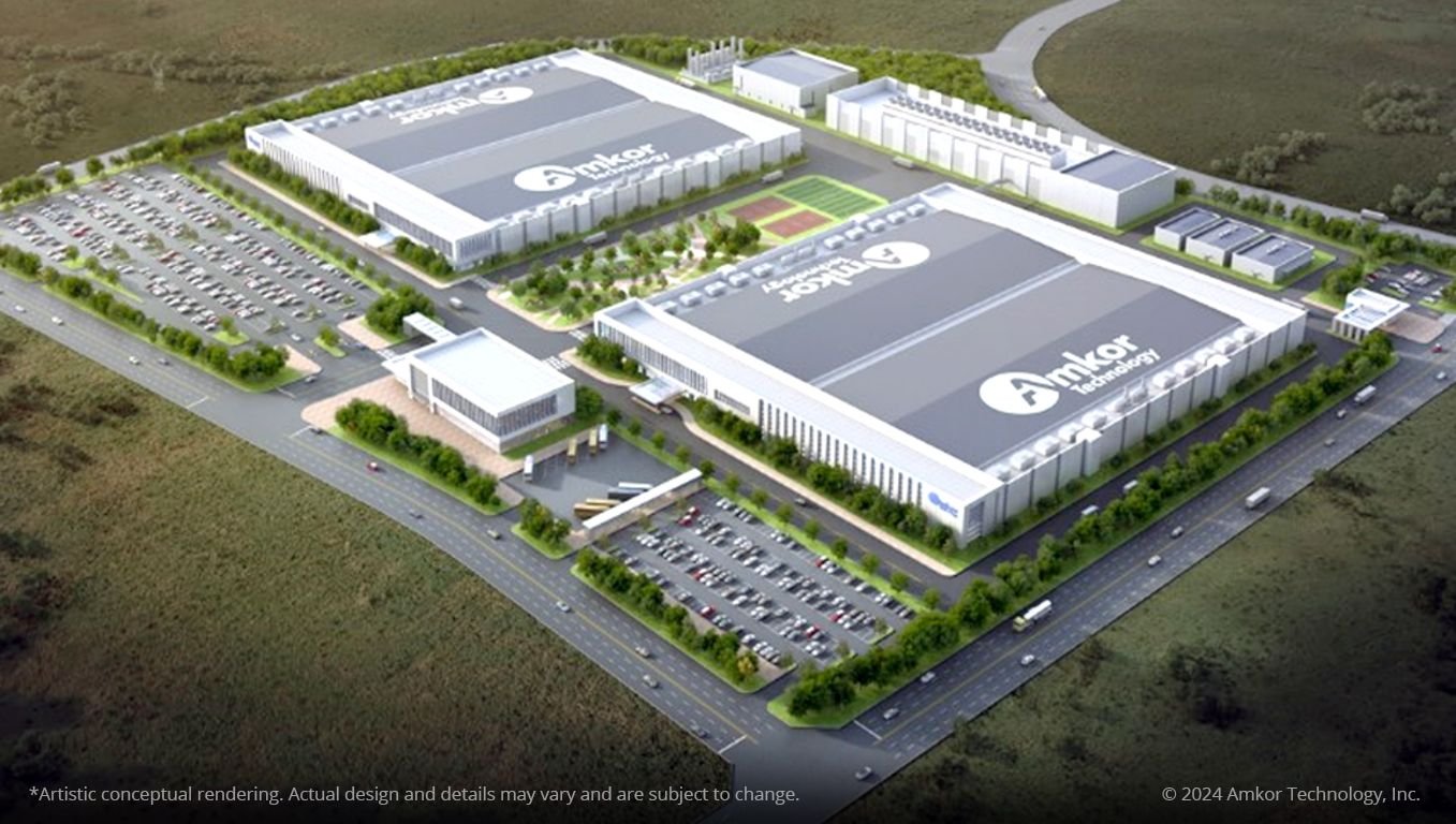
The US Department of Commerce has signed a non-binding preliminary memorandum of terms (PMT) with Amkor Technology to provide up to $400 million in proposed direct funding under the CHIPS and Science Act.
In addition to the proposed direct funding, an additional $200m in proposed loans will also be made available to Amkor from the CHIPS Program Office.

The proposed funding would be used to support Amkor’s $2 billion investment for an outsourced semiconductor assembly and test company (OSAT) plant in Peoria, Arizona.
In a statement, the department said the OSAT facility would be the largest of its type in the US and would create 2,000 jobs. While no completion date for the project has been announced yet, adding that the plant will “utilize the most advanced technology such as 2.5D technology and other next-generation technologies,” the final step in the manufacturing process for GPUs and AI chips.
“A lack of 2.5D technology capacity has been a significant chokepoint in the semiconductor industry’s ability to meet the rapidly increasing demand for generative AI products and services,” the Department of Commerce said.
In addition to creating new jobs in Peoria, Amkor has also committed to developing talent locally and across the US, partnering with Arizona State University, Grand Canyon University, Northern Arizona University, Maricopa Community College, Purdue University, and Western Maricopa Education Center.
“One of the fundamental goals of the CHIPS and Science Act is creating an advanced packaging ecosystem in the US to ensure full start-to-finish chip production occurs domestically. Advanced packaging drives chip innovation at all levels, and because of President Biden’s leadership, the US will have a robust domestic footprint in this critical technology,” said US Secretary of Commerce, Gina Raimondo. “The leading-edge chips that will be packaged right here in Arizona are foundational to technologies of the future that will define global economic and national security for decades to come.”
Giel Rutten, Amkor’s president and CEO, added: “Advanced packaging is an essential component of semiconductor innovation and manufacturing, and we appreciate our partners at the Department of Commerce for recognizing the importance of this sector as they work to support our industry.”
CHIPS Act funding shows no signs of slowing down
The $280bn CHIPS and Science Act was approved by Congress in July 2022, with $52bn of the overall funding package designated as subsidies for US semiconductor manufacturers. Funding from the act has also been earmarked for semiconductor R&D, growing a skilled semiconductor workforce, and incentives for the manufacturing of semiconductors and specialized tooling equipment.
In April, Commerce Secretary Gina Raimondo said she expected all the grant money under the CHIPS Act to be allocated by the end of this year.
To date, the White House has allocated the following funding:
- In February 2024, GlobalFoundries was awarded $1.5bn by the US government under the act to subsidize the company’s future semiconductor production capabilities and support expansion plans for its New York and Vermont sites.
- In March, it was announced that Intel would receive $8.5bn in direct funding, $11bn in low-interest rate loans, and a 25 percent investment tax credit on up to $100 billion of Intel’s capital investments under the Act. It will be used to support the company’s investments in Arizona, New Mexico, Ohio, and Oregon where the company is expanding its chipmaking facilities.
- In early April, TSMC signed an agreement with the US government in April that would see the company receive $11.6bn under the CHIPS and Science Act to build a third fabrication plant in Phoenix, Arizona. This newly announced TSMC fab will produce 2nm or “more advanced process technologies depending on customer demand” and is expected to be in production by the end of the decade.
- Also in April, it was announced that Samsung Electronics would receive $6.4bn in direct funding to build a semiconductor cluster across a number of locations in Texas. This includes two semiconductor foundries producing 4nm and 2nm chips; an advanced packaging facility for high memory bandwidth; a research and development facility in the city of Taylor, and the expansion of an existing Samsung site in Austin to support the production of fully depleted silicon-on-insulator (FD-SOI) process technologies.
- That same month, Micron was allocated up to $6.14bn in direct funding under the CHIPS and Science Act, which will be used to support the construction of three new memory chip fabs: Two in Clay, New York, and one in Boise, Idaho, which the company started construction on in 2023. The two fabs in Clay are the first of a planned four-fab “megafab” focused on DRAM (dynamic random-access memory) chip production, while the Boise facility will be a high-volume manufacturing (HVM) fab, also focused on the production of DRAM chips.
- In May, the US government allocated approximately $120m to Polar Semiconductor to support the expansion and modernization of the company’s manufacturing facility in Bloomington, Minnesota. The investment will allow Polar to double its production of sensor and power chips within two years and introduce new technology capabilities to the site.
- July saw the US Department of Commerce sign a non-binding preliminary memorandum of terms with Rogue Valley Microdevices (RVM) to provide up to $6.7m in proposed direct funding. Should it be granted, the money would be used to build a pure-play microelectromechanical system (MEMS) and sensor foundry facility in Palm Bay, Florida, in addition to bolstering the company’s operations in Oregon. RVM is the first women-and minority-owned business set to receive funding under the Act.
- That same month, the department also signed a non-binding preliminary memorandum of terms to provide Taiwanese silicon wafer supplier GlobalWafers with up to $400m in proposed direct funding under the CHIPS and Science Act. If the agreement moves forward, the funds would be used to establish the US’s first 300mm silicon wafer manufacturing facility for advanced chips in Sherman, Texas.


